I have found the following, as I have commented in github:
when debugging this problem, I am finding that if I make all of the contacts ohmic, and reverse the sign of the thermionic emission, that the simulation is now converging during the drain sweep.
So I feel that the convergence issue is partly fixed by reversing the sign on the thermionic emission. The next step would be to fix the schottky contacts.
Thanks for all your help,Juan!
I’m sorry that my previous programming habits were not good. I will separate my modified code and the original manuscript. I will separate out two .py ,“HEMT simulation” and “self-heating effects” , but this may need to be re-uploaded after this.
The second problem is the derivatives. Actually, I am not sure about the derivatives like the “Temperature:Holes@r1”. From a physical perspective, temperature changes will definitely affect the electrons, also holes. But when we solve the equations, they both set as variables. They should be independent, So, in previous tests, they were set to 0 by default which I think is reasonable. Of course, taking your advice, I would create corresponding node derivatives equal to 0. This is just my view, I am still a novice in the device simulation. Could it be understood this way, when two quantities do not show an explicit relationship in the program, the corresponding derivative can be set to 0?
I will try your changes about the “contact” and sign of thermionic emission.I may have confused the interface flux J_(⊥) and the direction of the corresponding current before. And I will continue to check the setting of “Schottkycontacts”.
The changes works, and the program now gives a converged calculation. But no current will be generated in the device. I am trying to figure out if there is still something wrong with the equilibrium carrier concentration I calculated on the Schottky contact interface.
Sorry, Juan. I made some mistakes on the dealing with the contact. Actually, the drain and source contact should set as Ohmic contact. I set a Schottky contact on them because I am trying to mimic the settings in the Silvaco example. In its example, the workfunc=3.93 is set on the drain and source contact. But actually, its barrier is equal to zero, which means a Ohmic contact. So for the contact in this simulation, only the gate should set as the Schottky contact.
The derivatives can be tricky. DEVSIM will look for derivatives with respect to each independent variable. The symbolic differentiator does not look at whether a model is independent before looking for a derivative.
I was just trying to suppress noise in the the output to the screen. It should have no effect on the run, because DEVSIM will assume that missing derivatives are already 0.
I make sign mistakes quite often, and I often find myself fixing them.
I am glad that you were able to make progress with your simulation. And I greatly appreciate you sharing your work. I have learned a lot.
Please let me know if you need any help understanding how DEVSIM works with the contact boundary conditions. These options to devsim.contact_equation determine the current flow:
Note that the node* models are integrated over the NodeVolume. I am thinking for your case, that it may be necessary to scale with ContactSurfaceArea/NodeVolume
if you need to account for the surface area of the contact.
Hello, Juan.
Thanks for your help and encourage! I learned a lot from the discussion and sharing in the forum. The setting of Schottky contact is referred to the sharing of QsChen: https://github.com/CQSim/QS-Devsim
Even though I wasn’t familiar with the devices he was working on, I could tell that he had done a very thorough simulation. I referred to his code when I was learning how to set up thermionic emission on the Schottky contact. But unfortunately, the calculation of the equilibrium carrier concentration of our work is not the same. And I am still not sure if my setting on the Schottky contact is right, especially the calculation of carrier equilibrium concentration. If you have time, may be you can help to check it.
Besides, I have create a new branch “Development” to distinguish my changes and original script. Now it should be easier for anyone to know what I am trying to do.
And still, the simulation faces some troubles, I can’t get the current because the 2DEG is not formed successfully. I am exploring if there is something wrong in the sheet charge, and if it could create the correct interface boundary which we have discussed.
I’d like to recommend a video about the 2DEG in HEMT: https://www.youtube.com/watch?v=KaAwKqYcfN0&t=100s
I may have misunderstood the work in an article ( Hao Q. International Journal of Heat and Mass Transfer, 2018, 116: 496-506.). In the TCAD simulation, the concentration of the two-dimensional electron gas should not be added to the sheet charge. By setting the polarization charge, the two-dimensional electron gas should come from the simulation.
Finally, I really appreciate your willingness to help me and discuss with me.
For the 2DEG, you may need to be looking for a quantum correction such as MLDA or density gradient. A classical simulator is not able to account for this effect without such corrections, as the classical simulation does not prevent charge from collecting at the surface.
The density gradient requires the calculation of 2 additional equations. I have an example here, for a MOSCAP:
Hi Juan and Ghost:
My net is not stable to connect to this forum. So I joined this discussion so late.
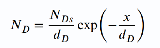
In my work about surface charge, I transfer the sheet charge density to bulk density by an exponential decay model with depth.
If you want to use this equation, just can add this node model of charge in the region on either side.
Hi QsChen, thanks for your kind suggestion. I tried it but I still couldn’t get the 2DEG. Could you please tell me how do you set the interface condition when the surface charge is existing in the interface?
Hi Ghost:
The interface between two semiconductor regions is so complicated. I’m still confused about it. But in the conversation between you and Juan, I have learned a lot.
Through my experience, the surface charge could be sorted into two types: carriers and traps.
For the carriers, you don’t need to treat them differently, just construct proper carriers and potential equations at the interface. The resenable sheet charge will be solved with proper equations. I think this will be the biggest challenge in your work.
For the traps, my method employs Ruler iteration to solve differential equations of trap generation and recombination with time. You should decide which side of the interface the tarp resides on.
Hi QsChen:
Sorry for so late to reply you. I’m appreciated that you shared your wonderful thoughts and experience. In past days, I am trying to simulate the heterojunction without surface charge.
GaN HEMT is not similar to the GaAS HEMT because of its special polarization charge. Since they are both heterojunctions devices, the similar energy band bending happens in the interface, and a certain two-dimensional electron gas will also form while the interface charge is not considered. After I introduced doping and made some changes, this part seemed to work, although I observed some strange things compared to commercial software (I’m going to ignore them for now).
As you say, the interface equation is my biggest challenge. In my view, the polarization charge is not similar to carriers. It is a bound charge and cannot move or generate current.
For the traps,I recently read the Sentaurus TCAD guide book, and it mentioned treating the polarization charges at the interface as fixed trap charges, but I can’t find more useful information or equations so far.
Judging from the most direct information I have found (already mentioned in the previous discussion), polarization charges will cause discontinuity of electric field in the interface . Do you have any experience setting relevant discontinuity in DEVSIM?
Hi Ghost:
I’m glad to hear that you have made some progress.
For the polarization charges, I modefiy the polarization in the Poisson equation: \nabla\bullet\ D=\rho_f. The displacement vector follow D= \varepsilon_0 E + P.
So in the ferroelectric materials, the polarization P could be calculated from history of field E.
The other method is modify the permittivity in the Poisson equation, in which the relative permittivity is calculated form the history of ield E. The commercial TCAD Tool Salvaco employ this apporach to simulate ferrelctcricity.
Tries to clarify how the displacement field behaves at an interface for an insulator (in the absence of any charge).
Adding a fixed charge, which is constant to an interface requires you to pick which side of the interface. If it is a volume charge, add it as an additional dopant to the Poisson equation. If it is a surface charge, then you would need to scale it by \text{SurfaceArea}/\text{NodeVolume}.
The continuous boundary condition would then ensure that the displacement vector follows the appropriate laws.
If the polarization charge is bias dependent, then you would need to track this dependence, perhaps by storing previous solution variables as suggested by @QsChen .
I think this video might be useful. It shows an example from process through device simulation. It also includes a quantum well for the 2D DEG. The device simulation starts at 8:30. It looks like they are solving traps at the interface and using a Schrodinger solver for the quantum well.
Hi Juan!
Thanks for your sharing and concern! In previous days, I could get the HEMT simulation under zero bias. And the results looked well, the potential, electrons concentration in 2DEG distribution is similar with the commercial TCAD (Same magnitude and distribution pattern, it is difficult to reproduce the exact same values but they are approximate). The band bending in the hetero-junction is simulated successfully, so I could get the 2DEG now. As for the quantum wall, I think it is not a necessary condition for the HEMT simulation. The classical DD model with out quantum corrections is also potential to simulate the hetero-junction devices.
I didn’t update the Git because I am trying to verify the I-V curve with commercial TCAD Silvaco. Actually, I could get the converged simulation under gate or drain sweep.However, current density is two orders of magnitude smaller in DEVSIM. The substrate shows a little leakage behavior. Maybe there is still something wrong in the code, I will update the repo in Git after I finished simulation and verify it successfully.