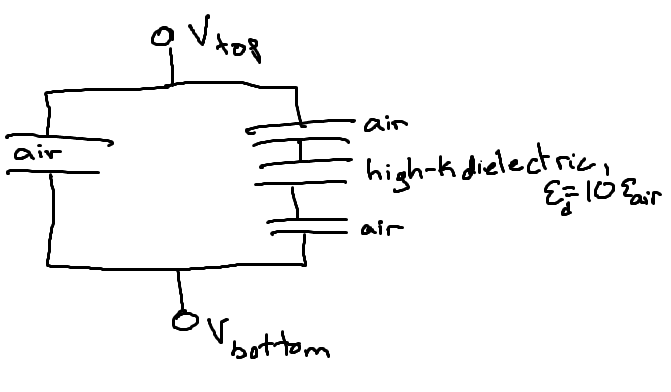
I don’t think that you’ve calculated the capacitance correctly - the structure I’ve defined has a half-slab of dielectric, so the full capacitor structure would be:
Full Code
from devsim import *
import numpy as np
import matplotlib
matplotlib.use('TkAgg')
from matplotlib import pyplot as plt
device="MyDevice"
region="MyRegion"
def cap2d():
'''
What is going on here? This forum post clears a lot up
https://forum.devsim.org/t/potential-and-electrical-field-definition/107
'''
device="MyDevice"
xmin, ymin = -100, -100 # window bottom left
xmax, ymax = 100, 100 # window top right
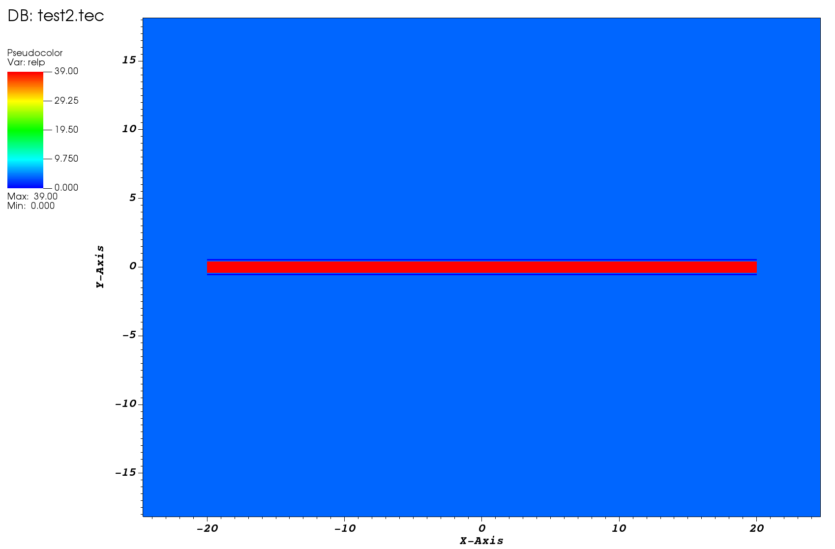
xlb, ylb = -20, -0.6 # bottom capacitor plate
xhb, yhb = 20, -0.5
xlt, ylt = -20, 0.5 # top capacitor plate
xht, yht = 20, 0.6
yl_di, yh_di, xl_di, xh_di = yhb+0.1, ylt-0.1, xlb, xhb #corners of dielectric layer
create_2d_mesh(mesh=device)
add_2d_mesh_line(mesh=device, dir="x", pos=xmin , ps=5)
add_2d_mesh_line(mesh=device, dir="x", pos=xmax , ps=5)
add_2d_mesh_line(mesh=device, dir="x", pos=xlt, ps=0.1)
add_2d_mesh_line(mesh=device, dir="x", pos=xht, ps=0.1)
add_2d_mesh_line(mesh=device, dir="x", pos=xlb, ps=0.1)
add_2d_mesh_line(mesh=device, dir="x", pos=xhb, ps=0.1)
add_2d_mesh_line(mesh=device, dir="x", pos=xl_di, ps=0.05)
add_2d_mesh_line(mesh=device, dir="x", pos=xh_di, ps=0.05)
add_2d_mesh_line(mesh=device, dir="y", pos=ymin , ps=5)
add_2d_mesh_line(mesh=device, dir="y", pos=ymax , ps=5)
add_2d_mesh_line(mesh=device, dir="y", pos=ylt, ps=0.1)
add_2d_mesh_line(mesh=device, dir="y", pos=yht, ps=0.1)
add_2d_mesh_line(mesh=device, dir="y", pos=ylb, ps=0.1)
add_2d_mesh_line(mesh=device, dir="y", pos=yhb, ps=0.1)
add_2d_mesh_line(mesh=device, dir="y", pos=yl_di, ps=0.05)
add_2d_mesh_line(mesh=device, dir="y", pos=yh_di, ps=0.05)
add_2d_region(mesh=device, material="gas" , region="air", yl=ymin, yh=ymax, xl=xmin, xh=xmax) #metal sits on the air
add_2d_region(mesh=device, material="metal", region="mb" , yl=ylb , yh=yhb , xl=xlb , xh=xhb)
add_2d_region(mesh=device, material="metal", region="mt" , yl=ylt , yh=yht , xl=xlt , xh=xht)
add_2d_region(mesh=device, material='gas', region='dielectric' , yl=yl_di , yh=yh_di , xl=xl_di , xh=xh_di)
# must be air since contacts don't have any equations
add_2d_contact(mesh=device, name="bot", region="air", material="metal", yl=ylb , yh=yhb , xl=xlb , xh=xhb)
add_2d_contact(mesh=device, name="top", region="air", material="metal", yl=ylt , yh=yht , xl=xlt , xh=xht)
add_2d_interface(mesh=device, name='air-dielectric', region0='dielectric', region1='air', yl=yl_di , yh=yh_di , xl=xl_di , xh=xh_di)
finalize_mesh( mesh=device)
create_device( mesh=device, device=device)
### Set parameters on the region
set_parameter(device=device, region='air', name="Permittivity", value=3.9*8.85e-14) #SiO2?
set_parameter(device=device, region='dielectric', name="Permittivity", value=39*8.85e-14)
for region in ('air', 'dielectric'):
### Create the Potential solution variable
node_solution(device=device, region=region, name="Potential")
### Creates the Potential@n0 and Potential@n1 edge model
edge_from_node_model(device=device, region=region, node_model="Potential")
### Electric field on each edge, as well as its derivatives with respect to the potential at each node
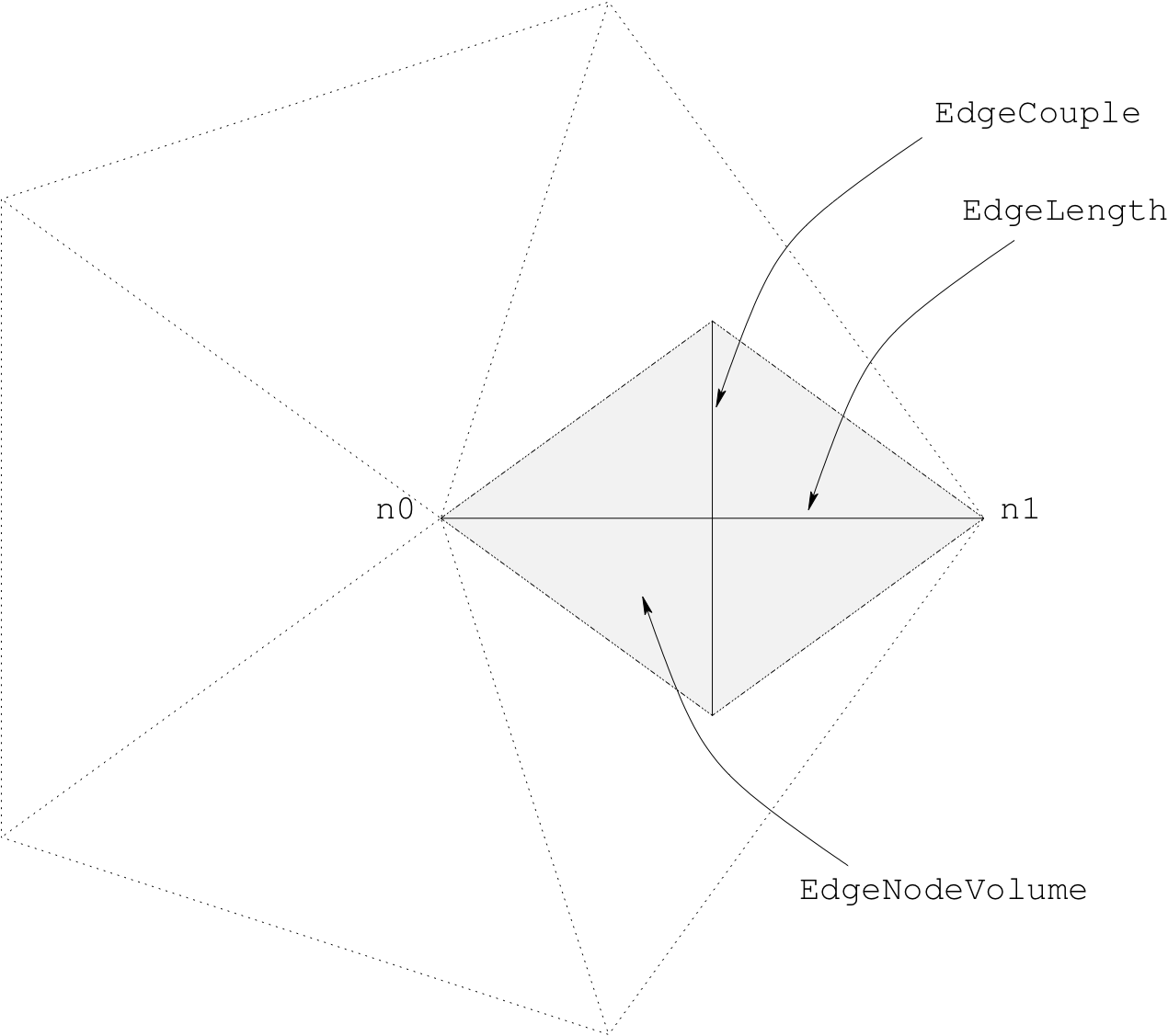
edge_model(device=device, region=region, name="ElectricField", equation="(Potential@n0 - Potential@n1)*EdgeInverseLength")
edge_model(device=device, region=region, name="ElectricField:Potential@n0", equation="+EdgeInverseLength")
edge_model(device=device, region=region, name="ElectricField:Potential@n1", equation="-EdgeInverseLength")
### Model the D Field
edge_model(device=device, region=region, name="DField", equation="Permittivity*ElectricField")
edge_model(device=device, region=region, name="DField:Potential@n0", equation="diff(Permittivity*ElectricField, Potential@n0)")
edge_model(device=device, region=region, name="DField:Potential@n1", equation="-DField:Potential@n0")
element_from_edge_model(device=device, region=region, edge_model="DField")
### Create the bulk equation
equation(device=device, region=region, name="PotentialEquation",
variable_name="Potential", edge_model="DField", variable_update="default")
# interface_normal_model(device=device, region=region, interface='air-dielectric')
interface_model( device=device, interface='air-dielectric', name='continuousP', equation='Potential@r0 - Potential@r1')
interface_model( device=device, interface='air-dielectric', name='continuousP:Potential@r0', equation='1')
interface_model( device=device, interface='air-dielectric', name='continuousP:Potential@r1', equation='-1')
interface_equation(device=device, interface='air-dielectric', name='PotentialEquation', interface_model='continuousP', type='continuous')
### Contact models and equations
for c in ("top", "bot"):
contact_node_model(device=device, contact=c, name=f"{c}_bc", equation=f"Potential - {c}_bias")
contact_node_model(device=device, contact=c, name=f"{c}_bc:Potential", equation="1")
contact_equation( device=device, contact=c, name="PotentialEquation",
node_model=f"{c}_bc", edge_charge_model="DField")
### Set the contact
set_parameter(device=device, name="top_bias", value=1e-0)
set_parameter(device=device, name="bot_bias", value=-1e-0)
edge_model(device=device, region="mb", name="ElectricField", equation="0") #E field is 0 in metal
edge_model(device=device, region="mt", name="ElectricField", equation="0")
node_model(device=device, region="mb", name="Potential", equation="bot_bias")
node_model(device=device, region="mt", name="Potential", equation="top_bias")
solve(type="dc", absolute_error=1.0, relative_error=1e-6, maximum_iterations=30, solver_type="direct")
element_from_edge_model(edge_model="ElectricField", device=device, region='air')
element_from_edge_model(edge_model="DField", device=device, region='air')
element_from_edge_model(edge_model="ElectricField", device=device, region='dielectric')
element_from_edge_model(edge_model="DField", device=device, region='dielectric')
print()
print(f'Calculated charge on top plate: {get_contact_charge(device=device, contact="top", equation="PotentialEquation")} C/cm')
V = (get_parameter(device=device, name="top_bias")-get_parameter(device=device, name="bot_bias"))
eps_air = get_parameter(device=device, region="air", name="Permittivity")
eps_die = get_parameter(device=device, region="dielectric", name="Permittivity")
w = (xht - xlt)/2 #half-width of the full capacitor structure
d_tb = ylt - yhb # length of gap between top and bottom plate
d_td = ylt - yh_di # " " top plate and top of dielectric
d_d = yh_di - yl_di # " " top of dielectric and bottom of dielectric
d_db = yl_di - yhb # " " bottom of dielectric and bottom plate
C_left = eps_air*w/d_tb #left capacitor is just air
C_topright = eps_air*w/d_td #top right capacitor, thin air layer
C_midright = eps_die*w/d_d #middle right capacitor, dielectric layer
C_botright = eps_air*w/d_db #bottom right capacitor, another thin air layer
C_right = ( C_topright**-1 + C_midright**-1 + C_botright**-1 )**-1 # right capacitor is air-dielectric-air
C_total = C_left + C_right #total capacitance
print(f'Expected charge on top plate: {C_total*V} C/cm') # C = \epsilon A/d, Q=CV
print(f'eps_die/eps_air={eps_die/eps_air}')
print('All capacitances in F/cm:')
print(f'C_topright={C_topright}, C_midright={C_midright}, C_botright={C_botright}')
print(f'C_left={C_left}, C_right={C_right}')
print(f'C_total={C_total}')
# print(get_contact_charge(device=device, contact="bot", equation="PotentialEquation"))
cap2d()
I really feel that the boundary condition is not correct. Can you explain your reasoning? There should be a charge layer at the dielectric interfaces, so Poisson’s equation should have a charge layer there.