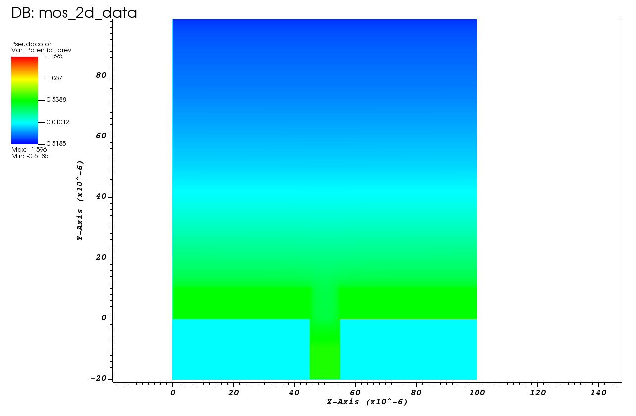
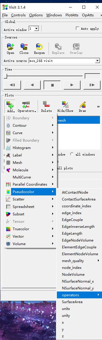
Hello, everyone! I am trying to learn the example of MOS2. But I can’t acquire a potential or carrier density distribution in the VISIT output file. I can only see the mesh in the VISIT. Below is the case file I used. Could anyone help me? Thank you.
mos_2d
# Copyright 2013 Devsim LLC
#
# Licensed under the Apache License, Version 2.0 (the "License");
# you may not use this file except in compliance with the License.
# You may obtain a copy of the License at
#
#     http://www.apache.org/licenses/LICENSE-2.0
#
# Unless required by applicable law or agreed to in writing, software
# distributed under the License is distributed on an "AS IS" BASIS,
# WITHOUT WARRANTIES OR CONDITIONS OF ANY KIND, either express or implied.
# See the License for the specific language governing permissions and
# limitations under the License.

import mos_2d_create
from mos_2d_physics import *

import devsim
device=devsim.get_device_list()[0]
oxide_regions   = ("oxide",)
silicon_regions = ("gate", "bulk")
all_regions     = ("gate", "bulk", "oxide")

for i in all_regions:
    createSolution(device, i, "Potential")

for i in silicon_regions:
    setSiliconParameters(device, i)
    createSiliconPotentialOnly(device, i)
for i in oxide_regions:
    setOxideParameters(device, i)
    createOxidePotentialOnly(device, "oxide")

createSiliconPotentialOnlyContact(device, "gate", "gate")
createSiliconPotentialOnlyContact(device, "bulk", "drain")
createSiliconPotentialOnlyContact(device, "bulk", "source")
createSiliconPotentialOnlyContact(device, "bulk", "body")

createSiliconOxideInterface(device, "bulk_oxide")
createSiliconOxideInterface(device, "gate_oxide")

devsim.solve(type="dc", absolute_error=1.0e-13, relative_error=1e-12, maximum_iterations=30)
devsim.solve(type="dc", absolute_error=1.0e-13, relative_error=1e-12, maximum_iterations=30)

createSolution(device, "gate", "Electrons")
createSolution(device, "gate", "Holes")
devsim.set_node_values(device=device, region="gate", name="Electrons", init_from="IntrinsicElectrons")
devsim.set_node_values(device=device, region="gate", name="Holes",     init_from="IntrinsicHoles")
createSiliconDriftDiffusion(device, "gate")
createSiliconDriftDiffusionAtContact(device, "gate", "gate")

createSolution(device, "bulk", "Electrons")
createSolution(device, "bulk", "Holes")
devsim.set_node_values(device=device, region="bulk", name="Electrons", init_from="IntrinsicElectrons")
devsim.set_node_values(device=device, region="bulk", name="Holes",     init_from="IntrinsicHoles")
createSiliconDriftDiffusion(device, "bulk")


createSiliconDriftDiffusionAtContact(device, "bulk", "drain")
createSiliconDriftDiffusionAtContact(device, "bulk", "source")
createSiliconDriftDiffusionAtContact(device, "bulk", "body")

devsim.solve(type="dc", absolute_error=1.0e30, relative_error=1e-5, maximum_iterations=30)

devsim.element_from_edge_model(edge_model="ElectricField", device=device, region="bulk")

devsim.write_devices(file="mos_2d_dd.msh", type="devsim")

with open("mos_2d_params.py", "w", encoding="utf-8") as ofh:
    ofh.write('import devsim\n')
    for p in devsim.get_parameter_list():
        v=repr(devsim.get_parameter(name=p))
        ofh.write('devsim.set_parameter(name="%s", value=%s)\n' % (p, v))
    for i in devsim.get_device_list():
        for p in devsim.get_parameter_list(device=i):
            v=repr(devsim.get_parameter(device=i, name=p))
            ofh.write('devsim.set_parameter(device="%s", name="%s", value=%s)\n' % (i, p, v))

    for i in devsim.get_device_list():
        for j in devsim.get_region_list(device=i):
            for p in devsim.get_parameter_list(device=i, region=j):
                v=repr(devsim.get_parameter(device=i, region=j, name=p))
                ofh.write('devsim.set_parameter(device="%s", region="%s", name="%s", value=%s)\n' % (i, j, p, v))

devsim.write_devices( file="mos_2dd", type="vtk")
mos_2d_physics
# Copyright 2013 Devsim LLC
#
# Licensed under the Apache License, Version 2.0 (the "License");
# you may not use this file except in compliance with the License.
# You may obtain a copy of the License at
#
#     http://www.apache.org/licenses/LICENSE-2.0
#
# Unless required by applicable law or agreed to in writing, software
# distributed under the License is distributed on an "AS IS" BASIS,
# WITHOUT WARRANTIES OR CONDITIONS OF ANY KIND, either express or implied.
# See the License for the specific language governing permissions and
# limitations under the License.

import devsim

def printCurrents(device, contact, bias):
    ecurr=devsim.get_contact_current(contact=contact, equation="ElectronContinuityEquation", device=device)
    hcurr=devsim.get_contact_current(contact=contact, equation="HoleContinuityEquation", device=device)
    tcurr = ecurr + hcurr
    print("%s %g %g %g %g" % (contact, bias, ecurr, hcurr, tcurr))

####
#### Constants
####
def setOxideParameters(device, region):
    q=1.6e-19
    k=1.3806503e-23
    eps=8.85e-14
    T=300
    devsim.set_parameter(device=device, region=region, name="Permittivity",   value=3.9*eps)
    devsim.set_parameter(device=device, region=region, name="ElectronCharge", value=q)

def setSiliconParameters(device, region):
    q=1.6e-19
    k=1.3806503e-23
    eps=8.85e-14
    T=300
    for name, value in (
        ("Permittivity", 11.1*eps),
      ("ElectronCharge", q),
      ("n_i", 1.0e10),
      ("kT", eps * T),
      ("V_t", k*T/q),
      ("mu_n", 400),
      ("mu_p", 200),
    ):
        devsim.set_parameter(device=device, region=region, name=name, value=value)

def createSolution(device, region, name):
    devsim.node_solution(device=device, region=region, name=name)
    devsim.edge_from_node_model(device=device, region=region, node_model=name)

def createSiliconPotentialOnly(device, region):
    ie = devsim.node_model(device=device, region=region, name="IntrinsicElectrons", equation="n_i*exp(Potential/V_t)")
    res = devsim.node_model(device=device, region=region, name="IntrinsicElectrons:Potential", equation="diff(%s, Potential)" % ie)
    for name, equation in (
        ("IntrinsicHoles",                         "n_i^2/IntrinsicElectrons"),
      ("IntrinsicHoles:Potential",               "diff(n_i^2/IntrinsicElectrons, Potential)"),
      ("IntrinsicCharge",                        "IntrinsicHoles-IntrinsicElectrons + NetDoping"),
      ("IntrinsicCharge:Potential",              "diff(IntrinsicHoles-IntrinsicElectrons, Potential)"),
      ("PotentialIntrinsicNodeCharge",           "-ElectronCharge*IntrinsicCharge"),
      ("PotentialIntrinsicNodeCharge:Potential", "diff(-ElectronCharge*IntrinsicCharge, Potential)"),
    ):
        devsim.node_model(device=device, region=region, name=name, equation=equation)

    for name, equation in (
        ("ElectricField",                  "(Potential@n0-Potential@n1)*EdgeInverseLength"),
      ("ElectricField:Potential@n0",     "EdgeInverseLength"),
      ("ElectricField:Potential@n1",     "-ElectricField:Potential@n0"),
      ("PotentialEdgeFlux",              "Permittivity*ElectricField"),
      ("PotentialEdgeFlux:Potential@n0", "diff(Permittivity*ElectricField,Potential@n0)"),
      ("PotentialEdgeFlux:Potential@n1", "-PotentialEdgeFlux:Potential@n0"),
    ):
        devsim.edge_model(device=device, region=region, name=name, equation=equation)

    devsim.equation(device=device, region=region, name="PotentialEquation", variable_name="Potential",
                    node_model="PotentialIntrinsicNodeCharge", edge_model="PotentialEdgeFlux", variable_update="log_damp")

def createSiliconPotentialOnlyContact(device, region, contact):
    bias_name="%sbias" % contact
    format_dict = { "contact" : contact}
    devsim.set_parameter(device=device, region=region, name=bias_name, value=0.0)
    for name, equation in (
        ("celec_%(contact)s", "1e-10 + 0.5*abs(NetDoping+(NetDoping^2 + 4 * n_i^2)^(0.5))"),
      ("chole_%(contact)s", "1e-10 + 0.5*abs(-NetDoping+(NetDoping^2 + 4 * n_i^2)^(0.5))"),
      ("%(contact)snodemodel", '''
        ifelse(NetDoping > 0,
          Potential-%(contact)sbias-V_t*log(celec_%(contact)s/n_i),
          Potential-%(contact)sbias+V_t*log(chole_%(contact)s/n_i))'''),
      ("%(contact)snodemodel:Potential", "1"),
    ):
        name_sub = name % format_dict
        equation_sub = equation % format_dict
        devsim.contact_node_model(device=device, contact=contact, name=name_sub, equation=equation_sub)

    devsim.contact_equation(device=device, contact=contact, name="PotentialEquation",
                            node_model="%snodemodel" % contact)

def createSiliconDriftDiffusion(device, region):
    for name, equation in (
        ("PotentialNodeCharge",           "-ElectronCharge*(Holes -Electrons + NetDoping)"),
      ("PotentialNodeCharge:Electrons", "+ElectronCharge"),
      ("PotentialNodeCharge:Holes",     "-ElectronCharge"),
    ):
        devsim.node_model(device=device, region=region, name=name, equation=equation)

    devsim.equation(device=device, region=region, name="PotentialEquation", variable_name="Potential", node_model="PotentialNodeCharge",
                    edge_model="PotentialEdgeFlux", variable_update="log_damp")

    createBernoulli(device, region)
    createElectronCurrent(device, region)
    createHoleCurrent(device, region)

    NCharge="-ElectronCharge * Electrons"
    dNChargedn="-ElectronCharge"
    devsim.node_model(device=device, region=region, name="NCharge", equation=NCharge)
    devsim.node_model(device=device, region=region, name="NCharge:Electrons", equation=dNChargedn)

    PCharge="-ElectronCharge * Holes"
    dPChargedp="-ElectronCharge"
    devsim.node_model(device=device, region=region, name="PCharge", equation=PCharge)
    devsim.node_model(device=device, region=region, name="PCharge:Holes", equation=dPChargedp)

    ni=devsim.get_parameter(device=device, region=region, name="n_i")
    devsim.set_parameter(device=device, region=region, name="n1", value=ni)
    devsim.set_parameter(device=device, region=region, name="p1", value=ni)
    devsim.set_parameter(device=device, region=region, name="taun", value=1e-5)
    devsim.set_parameter(device=device, region=region, name="taup", value=1e-5)

    USRH="-ElectronCharge*(Electrons*Holes - n_i^2)/(taup*(Electrons + n1) + taun*(Holes + p1))"
    dUSRHdn="simplify(diff(%s, Electrons))" % USRH
    dUSRHdp="simplify(diff(%s, Holes))" % USRH
    devsim.node_model(device=device, region=region , name="USRH", equation=USRH)
    devsim.node_model(device=device, region=region , name="USRH:Electrons", equation=dUSRHdn)
    devsim.node_model(device=device, region=region , name="USRH:Holes", equation=dUSRHdp)


    devsim.equation(device=device, region=region, name="ElectronContinuityEquation", variable_name="Electrons",
                    edge_model="ElectronCurrent", variable_update="positive",
                    time_node_model="NCharge", node_model="USRH")

    devsim.equation(device=device, region=region, name="HoleContinuityEquation", variable_name="Holes",
                    edge_model="HoleCurrent", variable_update="positive",
                    time_node_model="PCharge", node_model="USRH")

def createSiliconDriftDiffusionAtContact(device, region, contact):
    format_dict = { "contact" : contact }
    for name, equation in (
        ("%(contact)snodeelectrons",           "ifelse(NetDoping > 0, Electrons - celec_%(contact)s, Electrons - n_i^2/chole_%(contact)s)"),
      ("%(contact)snodeholes",               "ifelse(NetDoping < 0, Holes - chole_%(contact)s, Holes - n_i^2/celec_%(contact)s)"),
      ("%(contact)snodeelectrons:Electrons", "1.0"),
      ("%(contact)snodeholes:Holes",         "1.0"),
    ):
        name_sub = name % format_dict
        equation_sub = equation % format_dict
        devsim.contact_node_model(device=device, contact=contact, name=name_sub, equation=equation_sub)

    devsim.contact_equation(device=device, contact=contact, name="ElectronContinuityEquation",
                            node_model="%snodeelectrons" % contact, edge_current_model="ElectronCurrent")

    devsim.contact_equation(device=device, contact=contact, name="HoleContinuityEquation",
                            node_model="%snodeholes" % contact, edge_current_model="HoleCurrent")


def createOxidePotentialOnly(device, region):
    for name, equation in (
        ("ElectricField",                   "(Potential@n0 - Potential@n1)*EdgeInverseLength"),
      ("ElectricField:Potential@n0",      "EdgeInverseLength"),
      ("ElectricField:Potential@n1",      "-EdgeInverseLength"),
      ("PotentialEdgeFlux",               "Permittivity*ElectricField"),
      ("PotentialEdgeFlux:Potential@n0",  "diff(Permittivity*ElectricField, Potential@n0)"),
      ("PotentialEdgeFlux:Potential@n1",  "-PotentialEdgeFlux:Potential@n0"),
    ):
        devsim.edge_model(device=device, region=region, name=name, equation=equation)

    devsim.equation(device=device, region=region, name="PotentialEquation", variable_name="Potential",
                    edge_model="PotentialEdgeFlux", variable_update="log_damp")

def createSiliconOxideInterface(device, interface):
    for name, equation in (
        ("continuousPotential",              "Potential@r0-Potential@r1"),
      ("continuousPotential:Potential@r0", "1"),
      ("continuousPotential:Potential@r1", "-1"),
    ):
        devsim.interface_model(device=device, interface=interface, name=name, equation=equation)

    devsim.interface_equation(device=device, interface=interface, name="PotentialEquation", interface_model="continuousPotential", type="continuous")

def createSiliconSiliconInterface(device, interface):
    for variable in ("Potential", "Electrons", "Holes"):
        format_dict = { "var", variable }
        for name, equation in (
            ("continuous%(var)s", "%(var)s@r0-%(var)s@r1"),
          ("continuous%(var)s:%(var)s@r0", "1"),
          ("continuous%(var)s:%(var)s@r1", "-1"),
        ):
            name_sub = name % format_dict
            equation_sub = equation % format_dict
            devsim.interface_model(device=device, interface=interface, name=name_sub, equation=equation_sub)
        eqname = "%sEquation" % variable
        ieqname = "continuous%s" % variable
        devsim.interface_equation(device=device, interface=interface, name=eqname,
                                  interface_model=ieqname, type="continuous")

def createBernoulli(device, region):
    #### test for requisite models here
    vdiffstr="(Potential@n0 - Potential@n1)/V_t"
    for name, equation in (
        ("vdiff", vdiffstr),
      ("vdiff:Potential@n0",  "V_t^(-1)"),
      ("vdiff:Potential@n1",  "-vdiff:Potential@n0"),
      ("Bern01",              "B(vdiff)"),
      ("Bern01:Potential@n0", "dBdx(vdiff) * vdiff:Potential@n0"),
      ("Bern01:Potential@n1", "-Bern01:Potential@n0"),
      ("Bern10",              "Bern01 + vdiff"),
      ("Bern10:Potential@n0", "Bern01:Potential@n0 + vdiff:Potential@n0"),
      ("Bern10:Potential@n1", "Bern01:Potential@n1 + vdiff:Potential@n1"),
    ):
        devsim.edge_model(device=device, region=region, name=name, equation=equation)

def createElectronCurrent(device, region):
    Jn="ElectronCharge*mu_n*EdgeInverseLength*V_t*(Electrons@n1*Bern10 - Electrons@n0*Bern01)"
    devsim.edge_model(device=device, region=region, name="ElectronCurrent", equation=Jn)
    for variable in ("Electrons", "Potential"):
        der = "simplify(diff(%s, %s))" % (Jn, variable)
        devsim.edge_model(device=device, region=region, name="ElectronCurrent", equation=der)

def createHoleCurrent (device, region):
    Jp="-ElectronCharge*mu_p*EdgeInverseLength*V_t*(Holes@n1*Bern01 - Holes@n0*Bern10)"
    devsim.edge_model(device=device, region=region, name="HoleCurrent", equation=Jp)
    for variable in ("Holes", "Potential"):
        der = "simplify(diff(%s, %s))" % (Jp, variable)
        devsim.edge_model(device=device, region=region, name="HoleCurrent", equation=der)
mos_2d_create
# Copyright 2013 Devsim LLC
#
# Licensed under the Apache License, Version 2.0 (the "License");
# you may not use this file except in compliance with the License.
# You may obtain a copy of the License at
#
#     http://www.apache.org/licenses/LICENSE-2.0
#
# Unless required by applicable law or agreed to in writing, software
# distributed under the License is distributed on an "AS IS" BASIS,
# WITHOUT WARRANTIES OR CONDITIONS OF ANY KIND, either express or implied.
# See the License for the specific language governing permissions and
# limitations under the License.

import devsim
device="mymos"

device_width=   1.0e-4
gate_width=     1.0e-5
diffusion_width=0.4

air_thickness=      1e-7
oxide_thickness=    1e-5
gate_thickness=     1e-5
device_thickness=   1e-4
diffusion_thickness=1e-5

x_diffusion_decay=  1e-20
y_diffusion_decay=  1e-10

bulk_doping=        -1e15
body_doping=        -1e19
drain_doping=       1e19
source_doping=      1e19
gate_doping=        1e20

y_channel_spacing=    1e-8
y_diffusion_spacing=  1e-6
y_gate_top_spacing=   1e-8
y_gate_mid_spacing=   (gate_thickness * 0.25)
y_gate_bot_spacing=   1e-8
y_oxide_mid_spacing=  (oxide_thickness * 0.25)
x_channel_spacing=  1e-6
x_diffusion_spacing=1e-5
max_y_spacing=      1e-4
max_x_spacing=      1e-2
y_bulk_mid_spacing=(device_thickness * 0.25)
y_bulk_bottom_spacing=1e-8

x_bulk_left=  0.0
x_bulk_right= (x_bulk_left + device_width)
x_center=     (0.5 * (x_bulk_left + x_bulk_right))
x_gate_left=  (x_center - 0.5 * (gate_width))
x_gate_right= (x_center + 0.5 * (gate_width))
x_device_left=(x_bulk_left - air_thickness)
x_device_right=(x_bulk_right + air_thickness)

y_bulk_top=     0.0
y_oxide_top=    (y_bulk_top - oxide_thickness)
y_oxide_mid=    (0.5 * (y_oxide_top + y_bulk_top))
y_gate_top=     (y_oxide_top - gate_thickness)
y_gate_mid=     (0.5 * (y_gate_top + y_oxide_top))
y_device_top=   (y_gate_top - air_thickness)
y_bulk_bottom=  (y_bulk_top + device_thickness)
y_bulk_mid=     (0.5 * (y_bulk_top + y_bulk_bottom))
y_device_bottom=(y_bulk_bottom + air_thickness)
y_diffusion=    (y_bulk_top + diffusion_thickness)

devsim.create_2d_mesh(  mesh="mos")
devsim.add_2d_mesh_line(mesh="mos", dir="y", pos=y_device_top, ps=max_y_spacing)
devsim.add_2d_mesh_line(mesh="mos", dir="y", pos=y_gate_top, ps=y_gate_top_spacing)
devsim.add_2d_mesh_line(mesh="mos", dir="y", pos=y_gate_mid, ps=y_gate_mid_spacing)
devsim.add_2d_mesh_line(mesh="mos", dir="y", pos=y_oxide_top, ps=y_gate_bot_spacing, ns=y_oxide_mid_spacing)
devsim.add_2d_mesh_line(mesh="mos", dir="y", pos=y_oxide_mid, ps=y_oxide_mid_spacing)
devsim.add_2d_mesh_line(mesh="mos", dir="y", pos=y_bulk_top, ns=y_oxide_mid_spacing, ps=y_channel_spacing)
devsim.add_2d_mesh_line(mesh="mos", dir="y", pos=y_diffusion, ps=y_diffusion_spacing)
devsim.add_2d_mesh_line(mesh="mos", dir="y", pos=y_bulk_mid, ps=y_bulk_mid_spacing)
devsim.add_2d_mesh_line(mesh="mos", dir="y", pos=y_bulk_bottom, ns=y_bulk_bottom_spacing, ps=max_y_spacing)
devsim.add_2d_mesh_line(mesh="mos", dir="y", pos=y_device_bottom, ps=max_y_spacing)

devsim.add_2d_mesh_line(mesh="mos", dir="x", pos=x_center, ps=x_channel_spacing)
devsim.add_2d_mesh_line(mesh="mos", dir="x", pos=x_gate_left, ps=x_channel_spacing)
devsim.add_2d_mesh_line(mesh="mos", dir="x", pos=x_bulk_left, ps=x_diffusion_spacing)
devsim.add_2d_mesh_line(mesh="mos", dir="x", pos=x_gate_right, ps=x_channel_spacing)
devsim.add_2d_mesh_line(mesh="mos", dir="x", pos=x_bulk_right, ps=x_diffusion_spacing)
devsim.add_2d_mesh_line(mesh="mos", dir="x", pos=x_device_right, ps=max_x_spacing)
devsim.add_2d_mesh_line(mesh="mos", dir="x", pos=x_device_left, ps=max_x_spacing)

devsim.add_2d_region(mesh="mos", material="Air"    , region="air")
devsim.add_2d_region(mesh="mos", material="Silicon", region="bulk", xl=x_bulk_left, xh=x_bulk_right, yl=y_bulk_bottom, yh=y_bulk_top)
devsim.add_2d_region(mesh="mos", material="Silicon", region="gate", xl=x_gate_left, xh=x_gate_right, yl=y_oxide_top, yh=y_gate_top)
devsim.add_2d_region(mesh="mos", material="Oxide"  , region="oxide", xl=x_gate_left, xh=x_gate_right, yl=y_bulk_top, yh=y_oxide_top)

devsim.add_2d_contact(mesh="mos", name="gate", region="gate", yl=y_gate_top, yh=y_gate_top, material="metal")
devsim.add_2d_contact(mesh="mos", name="body", region="bulk", yl=y_bulk_bottom, yh=y_bulk_bottom, material="metal")
devsim.add_2d_contact(mesh="mos", name="source", region="bulk", yl=y_bulk_top, yh=y_bulk_top, xl=x_device_left, xh=x_gate_left, material="metal")
devsim.add_2d_contact(mesh="mos", name="drain" , region="bulk", yl=y_bulk_top, yh=y_bulk_top, xl=x_gate_right, xh=x_device_right, material="metal")

devsim.add_2d_interface(mesh="mos", name="gate_oxide", region0="gate", region1="oxide")
devsim.add_2d_interface(mesh="mos", name="bulk_oxide", region0="bulk", region1="oxide")
devsim.finalize_mesh(mesh="mos")
devsim.create_device(mesh="mos", device=device)


format_dict= {
    'gate_doping' : gate_doping,
  'source_doping' : source_doping,
  'drain_doping' : drain_doping,
  'body_doping' : body_doping,
  'bulk_doping' : bulk_doping,
  'x_gate_left' : x_gate_left,
  'x_gate_right' : x_gate_right,
  'x_diffusion_decay' : x_diffusion_decay,
  'y_diffusion' : y_diffusion,
  'y_diffusion_decay' : y_diffusion_decay,
  'y_bulk_bottom' : y_bulk_bottom,
}

devsim.node_model(name="NetDoping"   , device=device, region="gate", equation="%(gate_doping)s" % format_dict)
devsim.node_model(name="DrainDoping" , device=device, region="bulk", equation="0.25*%(drain_doping)s*erfc((x-%(x_gate_left)s)/%(x_diffusion_decay)s)*erfc((y-%(y_diffusion)s)/%(y_diffusion_decay)s)" % format_dict)
devsim.node_model(name="SourceDoping", device=device, region="bulk", equation="0.25*%(source_doping)s*erfc(-(x-%(x_gate_right)s)/%(x_diffusion_decay)s)*erfc((y-%(y_diffusion)s)/%(y_diffusion_decay)s)" % format_dict)
devsim.node_model(name="BodyDoping", device=device, region="bulk", equation="0.5*%(body_doping)s*erfc(-(y-%(y_bulk_bottom)s)/%(y_diffusion_decay)s)" % format_dict)
devsim.node_model(name="NetDoping"   , device=device, region="bulk", equation="DrainDoping + SourceDoping + %(bulk_doping)s + BodyDoping" % format_dict)

devsim.write_devices( file="mos_2d", type="vtk")
devsim.write_devices( file="mos_2d.flps", type="floops")