Material name in gmsh and periodic boundaries

Hi!

Thanks for making this tool available to the broader community. It’s a great piece of SW.

I’m trying to follow the diode example but with an external 3D mesh generated with gmsh.

I have two initial questions when doing this:

  1. The command add_gmsh_region() takes in the argument material. In simple_physics there’s not mention of the material except for the constants (relative permittivity). Would I be right if I say that the material name is irrelevant when calling add_gmsh_region() as long as I make sure that the constants in simple_physics are adjusted appropriately?
  2. If I define some periodic BCs in gmsh, do I need to define these with add_gmsh_interface?

Thanks a lot in advance.

Welcome to the forum!

The material value does not affect anything. It can be anything you want, and it can be queried using this command:
https://devsim.net/CommandReference.html#devsim.get_material

There is some periodic BC support available. Please see this section:
https://devsim.net/meshing.html#periodic-boundary-conditions
https://devsim.net/CommandReference.html#devsim.create_interface_from_nodes

This command would be issued after the device has been created.

Note that the documentation is rather limited, but involved identifying nodes on both sides of your device to attach together. I’d consider it experimental work that I had done for @Johan_Lauwaert.

I might be able to provide a script, in 2d, that I used before to identify matched nodes in gmsh, so please let me know if this would be useful to you.

Here is some code for a periodic BC work I had done for someone. It treats the left and right boundary conditions as contacts when creating the 2D device.

The get_matching_nodes function matches up the nodes on the sides of the device.

def get_matching_nodes():
    left_elements = get_element_node_list(device=device, region='PU', contact='left')
    right_elements = get_element_node_list(device=device, region='PU', contact='right')
    ypos = get_node_model_values(device=device, region='PU', name='y')
    left_nodes = set([])
    right_nodes = set([])
    [left_nodes.update(i) for i in left_elements]
    [right_nodes.update(i) for i in right_elements]
    print(left_nodes)
    print(right_nodes)
    left_nodes = sorted(left_nodes, key=lambda x: (ypos[x]))
    right_nodes = sorted(right_nodes, key=lambda x: (ypos[x]))
    #print([ypos[x] for x in left_nodes])
    #print([ypos[x] for x in right_nodes])
    for i, j in zip(left_nodes, right_nodes):
        print(ypos[i], ypos[j])
    return {
      'device' : device,
      'name' : 'pbc',
      'region0' : 'PU',
      'region1' : 'PU',
      'nodes0' : left_nodes,
      'nodes1' : right_nodes,
    }

create_gmsh_mesh(file="Periodic4_withoutInfo.msh", mesh="heat")
add_gmsh_region(mesh="heat", gmsh_name="staal", region="staal", material="staal")
.
.
.
add_gmsh_contact(mesh="heat", gmsh_name="left", region="PU", name="left", material="metal")
add_gmsh_contact(mesh="heat", gmsh_name="right", region="PU", name="right", material="metal")

finalize_mesh(mesh="heat")
create_device(mesh="heat", device=device)

pbc = get_matching_nodes()
create_interface_from_nodes(**pbc)

Thanks a lot for your prompt response!

Additionally, I’m assuming one doesn’t require do anything with free surfaces, right?

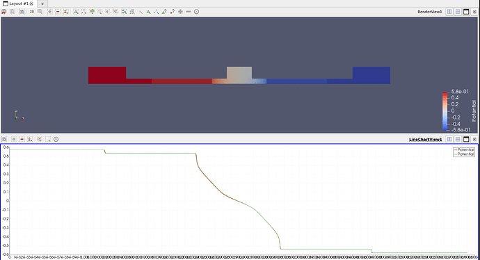
I have been able to run a 3D simulation and compare it against the same in 2D. Unfortunately, I haven’t been able to understand why the BC isn’t being applied. In my script I have

devsim.set_parameter(device="device", name=simple_physics.GetContactBiasName(new_name), value=bias)
simple_physics.CreateSiliconPotentialOnlyContact(device="device", region=zone, contact=new_name)

This is the result:

The lines in the figure are Potential for the 2D (brown) and 3D (green) cases. Both are very close to each other but they don’t comply with my bias, which I have set to 0.

I’m also including some output:

...
Region zone_8 has 1658 nodes.
Region zone_9 has 7699 nodes.
Contact zone_5_bc_5 in region zone_5 with 132 nodes
Contact zone_9_bc_9 in region zone_9 with 132 nodes
Adding interface zone_1_bc_0 with 33, 33 nodes
Adding interface zone_1_bc_1 with 33, 33 nodes
...

and later

Warning: Replacing equation with equation of the same name.
Region: zone_1, Equation: PotentialEquation, Variable: Potential
Warning: Replacing equation with equation of the same name.
Region: zone_2, Equation: PotentialEquation, Variable: Potential
Warning: Replacing equation with equation of the same name.
Region: zone_3, Equation: PotentialEquation, Variable: Potential
Warning: Replacing equation with equation of the same name.
Region: zone_4, Equation: PotentialEquation, Variable: Potential
Warning: Replacing equation with equation of the same name.
Region: zone_5, Equation: PotentialEquation, Variable: Potential
Warning: Replacing equation with equation of the same name.
Region: zone_6, Equation: PotentialEquation, Variable: Potential
Warning: Replacing equation with equation of the same name.
Region: zone_7, Equation: PotentialEquation, Variable: Potential
Warning: Replacing equation with equation of the same name.
Region: zone_8, Equation: PotentialEquation, Variable: Potential
Warning: Replacing equation with equation of the same name.
Region: zone_9, Equation: PotentialEquation, Variable: Potential

Maybe the BC not being forced is the results of these warnings?
Hi @MbolGi,

The warnings are from switching from the the Potential only equation to the drift-diffusion system of equations.

For a 0 bias ohmic contact, you can calculate the internal potential based on the net doping. The assumption is zero net charge at equilibrium

p - n - N_A + N_D = 0

where

p = n_i^2/n = n_i \exp(\frac{\psi}{V_T})

or

n = n_i^2 / p = n_i \exp(\frac{-\psi}{V_T})

The potential \psi is fixed at the ohmic contact and is a measure of how far the intrinsic Fermi level has been moved from the center of the bandgap by the 0 net charge condition above.

\psi = \frac{E_i - E_F}{q}

I apologize in advance if some of the signs do not make sense. Please see here for the relevent code.
CreateSiliconPotentialOnlyContact

Please make sure that these conditions make sense for your doping profile.

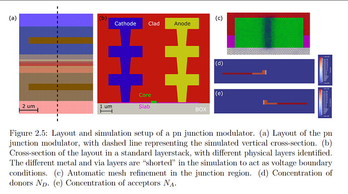
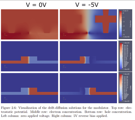
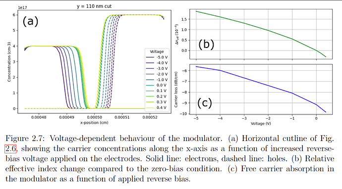
@MbolGi as an aside since I saw your nice figure above, I also have a silicon photonic modulator example over at GitHub - simbilod/gdevsim at dev in case you are interested, specifically gdevsim/docs/examples/optoelectronic/modulator.py at dev · simbilod/gdevsim · GitHub

It takes in a GDS and descriptions of the layers (including doping profiles) to setup the simulation and refine the mesh, then computes the charge vs voltage, and perturbs a mode calculated with a finite-element solver on the same mesh to calculate phase shift and absorption.

I still need to make all these doc pages look good before I push to main, but maybe the script is useful to you.

Some plots:


@Juan in principle this can take any GDS so I was hoping to make examples with transistors, but I was to busy wrapping up my thesis

Thanks @Juan for your detailed reply.

I modified the contact model in this manner:

\psi = V_i,
p+n-N_A+N_D = 0, and pn = n_{i}^{2}

Basically, I set the potential to V_i and then I enforce charge neutrality (the solutions to n and p depend on the sign of the net charge). Results are now what I want, however, would that approach be too naive?

Hi @simbilod,

This is a very interesting work. I’ll be definitely looking into this more in detail in the coming days/weeks.

Many thanks!

Hi @MbolGi

Your equations look good to me. There are more advanced models, but it really depends on your application as to whether they are warranted.

Here is an interesting paper that discusses when you might reconsider the use of the intrinsic Fermi level:

1 Like

This is exciting. Please send me a link to your thesis when it is published.

1 Like

Hi @Juan ,

while looking in simple_physics I realized that the equation PotentialEquation with variable name Potential is defined twice with different node/edge models. When this happens, does one equation replace the other?

Many thanks,
Marc

Yes, the equation is fully replaced. The potential only solution is used to create an initial guess for the drift-diffusion equation system. Solving drift diffusion at equilibrium does not usually converge without a reasonable initial guess.

You can use devsim.delete_equation

if you would like to delete the PotentialEquation before redefining it.

1 Like

Thanks @Juan,

I’m now trying to replicate simple_physics for my own simulations but get this error:

Invalid argument while evaluating function kahan3
while evaluating node model PotentialNodeCharge on Device: device on Region: zone_1
Value for "Holes" not available.
Value for "Electrons" not available.

Since Holes and Electrons have been created I guess my question is: when are the models evaluated?

Many thanks

Hi,

From the diode example files there is a function available:
DriftDiffusionInitialSolution

def DriftDiffusionInitialSolution(device, region, circuit_contacts=None):
    ####
    #### drift diffusion solution variables
    ####
    CreateSolution(device, region, "Electrons")
    CreateSolution(device, region, "Holes")

    ####
    #### create initial guess from dc only solution
    ####
    set_node_values(
        device=device, region=region, name="Electrons", init_from="IntrinsicElectrons"
    )
    set_node_values(
        device=device, region=region, name="Holes", init_from="IntrinsicHoles"
    )

    ###
    ### Set up equations
    ###
    CreateSiliconDriftDiffusion(device, region)
    for i in get_contact_list(device=device):
        if circuit_contacts and i in circuit_contacts:
            CreateSiliconDriftDiffusionAtContact(device, region, i, True)
        else:
            CreateSiliconDriftDiffusionAtContact(device, region, i)

It is good to create Electrons and Holes before using them in model equations. Otherwise the parser will treat the names as parameters instead of models, and won’t be able to find them.

1 Like