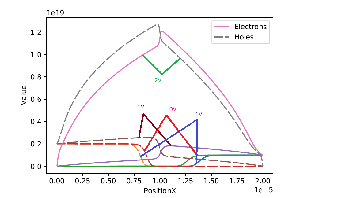
For the reverse biased condition, the space charge region expands with bias.
Under low positive bias, the width of space charge region grows narrower.
But while the bias over 1V, the carriers density for both electron and hole
increasing obversely.
I doubt this result. Whether the real diode should present such a scene?
It is quite possible this is not a physical result, when you are at such a high bias. If this is a silicon, with a bandgap of 1.12 eV, then applying a 2V bias would put you in some form of high injection:
At the moment, I am not sure how the physical models would need to be modified. The mesh may need to be refined, or the structure may need to be made longer.
The electron and hole densitiies are pinned at the ideal ohmic contact, so that:
p - n + N_D - N_A = 0
p = n_{i}^2/n
In addition, the continuity equations may need to be updated for Fermi statistics, instead of Boltzmann.